
[ad_1]
One of the key semiconductor technologies beyond 3D FinFET transistors are Gate-All-Around transistors, which show promise in helping to expand the ability to drive processors and components to higher performance and higher performance. lower power. Samsung has always announced that its first generation GAA technology will align with its “3nm” nodes, with its 3GAE and 3GAP processes. As part of today’s Samsung Foundry Forum, additional information was provided on the rollout schedule, as well as its 2nm process.
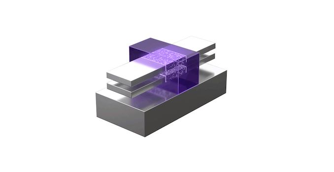
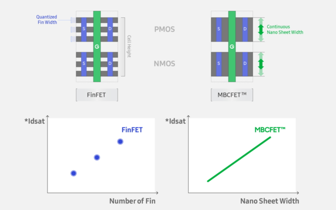
It has been widely predicted that once the standard FinFET runs out, the semiconductor manufacturing industry will pivot to GAAFET designs. Each of the leading vendors calls their implementation something different (RibbonFET for Intel, MBCFET for Samsung), but all use the same basic principle – a flexible-width transistor with a number of layers helping to drive the current of the transistor. Where FinFETs rely on multiple quantized fins for source / drain and a cell height of multiple fin tracks, GAAFETs allow a single fin of variable length, allowing the current to be optimized for each individual cellular device in terms of power, performance or surface.
All major vendors have been discussing GAAFETs at semiconductor technical conferences for several years. For example, at the VLSI international conference in June 2020, Intel CTO Dr. Mike Mayberry presented a diagram with the improved electrostatics of moving to a GAA design. At the time, we asked about Intel’s timeline for implementing GAA in volume, and we were told to expect them to be “within 5 years.” Currently, Intel’s RibbonFET is expected to ship with the 20A process, which is expected to be produced by the end of 2024. TSMC, on the other hand, is introducing its equivalent technology with its 2nm process nodes, stating that they can extend the life of their FinFET technology to another generation in 3nm. The exact timing of TSMC’s deployment is still quite unclear at this point, as the company expects its N5 and N3 offerings to be extended nodes with long lifetimes.
Samsung actually surprised us a few years ago, announcing that it had a prototype version of its GAA technology in early 2019. The company said it is shipping its v0.1 SDK to its partners, allowing them to experience the first design rules required by Samsung. This has improved over time, and during a presentation a few months ago at a China-only conference, the company said that a version of its 3nm GAA technology would be on track for the deployment in 2022. Today, Samsung confirms and extends these expectations.

Speaking to Samsung’s MoonSoo Kang, Samsung’s senior vice president of foundry market strategy, he described the following timeline for Samsung’s GAA process nodes:
- 3GAE will enter mass production by EoY 2022
- 3GAP will follow in a year for mass production at EoY 2023
- 2GAP will take a few more years, mass production in 2025
He added the caveat that these are mass production schedules – the product on the shelves will depend on customers and their own deployments. From that, we usually add one or two quarters (3-6 months) after these hours, so 2GAP is realistically a 2026 product for end users based on these times.
This is the first time Samsung has talked about its 2nm process technology, and it comes across as an iterative optimization with what Samsung expects to deliver with the 3nm variants. Exact details on the expected performance of these process nodes can be presented later today at the Samsung Foundry Forum 2021 event. Stay tuned for additional coverage.

[ad_2]
Source link