
[ad_1]
An executive who visits various research divisions around the world isn’t necessarily new, but with a focus on social media to drive appointees in every company to keep their followers sitting on the edge of their seats, it does. means we get a lot more information about how these companies operate. The downside to posting to social media is that some images exposing unpublished information are not verified by public relations or legal, and we get a glimpse of the next generation of technology. This is what happened today.
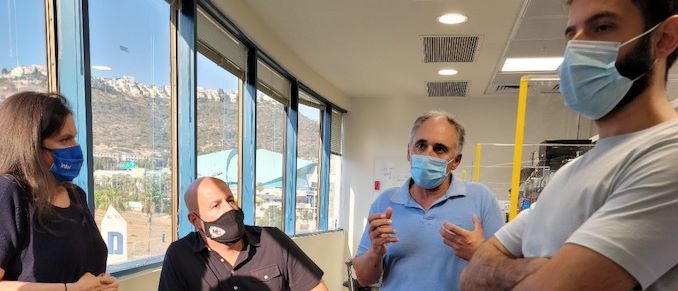
Day 1 with the @intel The Israel team in the books. Great views… amazing opp to see @GetThunderbolt innovation… a visit to the validation lab and time with the team… I can’t wait to see what tomorrow has in store! pic.twitter.com/GKOddA6TNi
– Gregory M Bryant (@gregorymbryant) August 1, 2021
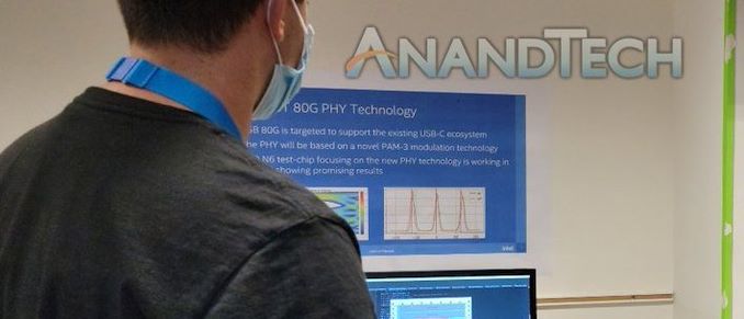
Executive Vice President and General Manager of Intel’s Customer Computing Group, Gregory Bryant, is spending this week at Intel’s R&D facilities in Israel on his first overseas trip with Intel in 2021. A first Sunday morning’s article, featuring Bryant’s trip to the gym to overcome jet lag, was followed by another later in the day, with Bryant being shown the desks and research. The post contained four photos, but was quickly deleted and replaced with a photo with three (in the tweet above). The deleted photo features new information about next-generation Thunderbolt technology.
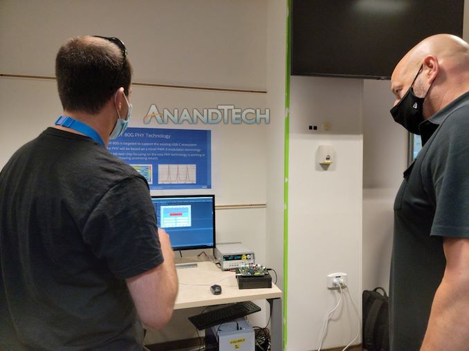
In this image we can see a poster on the wall featuring ‘PHY 80G technology‘, which means that Intel is working on a physical layer (PHY) for 80 Gbit / s connections. Initially, this is double the bandwidth of Thunderbolt 4, which operates at 40 Gbps.
The second line confirms that it is’USB 80G is intended to support the existing USB-C ecosystem‘, which follows the fact that Intel aims to keep the USB-C connector but to double the effective bandwidth.
The third line is actually where it gets technically interesting. ‘The PHY will be based on the new PAM-3 modulation technology‘. This is the way 0s and 1s are transmitted – traditionally we are talking about NRZ encoding, which simply allows a 0 or a 1, or a single bit to be transmitted. Natural progression is a pattern for transferring two bits, and it’s called PAM-4 (Pulse Amplitude Modulation), with 4 being the demarcation for how many different variants two bits could be seen (either 00, 01, 10, or 11). PAM-4, at the same frequency, therefore has 2x the bandwidth of an NRZ connection.
So what in PAM-3?
By Teledyne LaCroy on YouTube
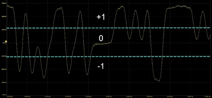
PAM-3 is a technology where the data line can carry a -1, a 0 or a +1. The system actually combines two PAM-3 transmissions into a 3-bit data signal, such that 000 is a -1 followed by a -1. It gets complex, so here is a table:
| PAM-3 encoding | ||
| AnandTech | To transmit 1 |
To transmit 2 |
| 000 | -1 | -1 |
| 001 | -1 | 0 |
| 010 | -1 | 1 |
| 011 | 0 | -1 |
| 100 | 0 | 1 |
| 101 | 1 | -1 |
| 110 | 1 | 0 |
| 111 | 1 | 1 |
| Unused | 0 | 0 |
When we compare NRZ to PAM-3 and PAM-4, we can see that the data transfer rate for PAM-3 is in the middle of NRZ and PAM-4. The reason PAM-3 is used in this case is to achieve this higher bandwidth without the additional limitations that PAM-4 needs to be activated.
| NRZ vs. PAM-3 vs. PAM4 | |||
| AnandTech | Parts | Cycles | Bits by Cycle |
| NRZ | 1 | 1 | 1 |
| PAM-3 | 3 | 2 | 1.5 |
| PAM-4 | 2 | 1 | 2 |
PAM-3 has limitations similar to NRZ.
The last line of this image is’[something] New PHY technology focused N6 test chip works in [the lab and] showing promising results‘. That first word I thought was TSMC, but it must be roughly the same width as the “The” on the line above. So it doesn’t seem like I’m there, but N6 is a TSMC node.
Intel’s goal with Thunderbolt will be to both improve bandwidth, power, and utility, but it also looks like at this point in time it looks like keeping the USB-C standard is going to be. an essential part of keeping the technology useful for users who can fall back on standard USB-C connections. Right now Intel’s TB4 is a superset that includes USB4, so we might see another situation where TB5 is also set to be a superset of USB5, but it looks like the USB standards are slower to deploy than TB standards at this time.
Special thanks to David Schor from WikiChip for the tip.
Related reading
[ad_2]
Source link