
[ad_1]
&ball; Physics 12, 93
A law describing the attenuation of electrons in solids has long been helping researchers determine the size of objects at the nanoscale, but experiments show that it is less general than one does. thought it before.

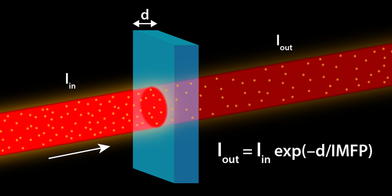
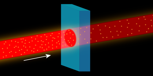
In science and technology at the nanoscale, it is of utmost importance to be able to measure the dimensions of an object with nanoscale precision. Scanning probe microscopy is the most accurate tool for determining the lateral dimensions of patterns on a surface. Along the vertical coordinate, the dimensions can be deduced from the fact that an incoming electron beam is attenuated according to the thickness of the material (Fig. 1). Over the last 50 years, researchers have thought that a universal law could be used to convert the attenuation factors of electrons into thicknesses for a wide range of electronic energies (see note in ref. [1]). However, the law has barely been tested for low energies (1 to 50 eV), a range of increasing scientific and technological importance. Now, Daniël Geelen of the University of Leiden in the Netherlands and his collaborators have characterized the propagation of electrons through multilayer graphene at these energies, showing clear deviations from the expected universal behavior. [2]. Their analysis indicates that the attenuation of the electron beam is significantly affected by the solid band structure and therefore depends on the material. The result will benefit the quantitative understanding of many techniques using low energy electron beams, including photoemission, microscopy, diffraction, and electron beam lithography.
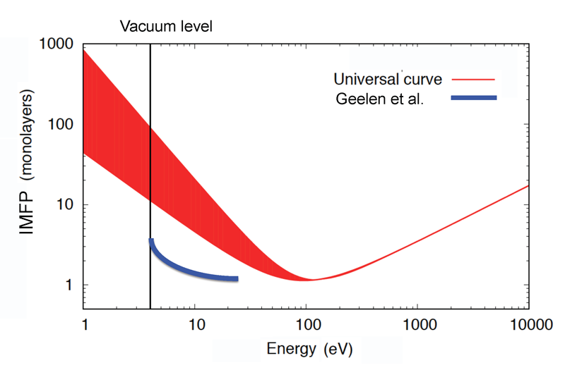
The universal law connects the energy of electrons to the trajectory with no mean inelastic average electron (IMFP), the average length over which the electron moves before losing energy when it 's time. a broadcasting event. In 1979, two researchers compiled data on the attenuation length of electrons (see note in ref. [3]) and concluded that the PIPF follows a universal curve, with negligible dependence on the specific material [4]. According to their law, this characteristic length reaches its minimum value – about one atomic layer – at about 50 eV (Fig. 2). This behavior reflects the energy dependence of different mechanisms of loss of electronic energy. The excitation of the phonons and the transitions between the electronic bands of the solid dominate in the field of low energies. Coupling to collective modes (plasmons) plays an important role at slightly higher energies, setting the minimum at about 50 eV. Above 50 eV, the increase in the IMFP reflects, vaguely, the reduction in interaction time: faster electrons have less time to be broadcast by the I & # 39; sample.
W. Werner / TU Wien

As shown in FIG. 2., The IMFP remains shorter than a few hundred atomic layers over a wide range of energy (1 to 10,000 eV), which is why electron beam attenuation is a measurement of thickness as sensitive. Researchers agree on values to use for the energies above 100 eV [5]and have largely adopted a 2015 formula describing the energy dependence of the PIMF above 50 eV [6]. For energies below 50 eV, however, a great deal of uncertainty persists (Fig. 2), mainly because of two causes. The first is a serious shortage of experimental data in this energy range. Working with eV electrons is a challenge because they are difficult to focus and their trajectories can be affected by small magnetic fields in the environment, including that of the Earth. In addition, PIPF is difficult to measure because it is so small and experiments require carefully controlled samples. The second is that, from a theoretical point of view, it is not clear how to treat the damping of collective oscillations of plasmon at these energies. [7].
Geelen and his collaborators have been able to characterize the propagation of low energy electrons through multilayer graphene (one to four atomic layers). Drawing on the latest technological advances, the team used a transmission electron microscope (TEM) and a previously developed low-energy electron microscope. [8] measure respectively the transmitted and reflected intensity of the electrons striking the samples with energies between 4 and 25 eV. From such intensities, they have not only deduced the IMFP, but also the average elastic path, the average length over which the electrons are scattered without loss of energy. Their measured values for the PIPM are almost 10 times lower than could be predicted with the universal law.
This gap with respect to universality is similar to that suggested by data from a 2013 study [8], which were based solely on electronic thinking. However, by characterizing the pathway without elastic means by simultaneous reflection and transmission measurements, the authors could explore the reasons for this behavior. Strikingly, they found that the path without elastic means at certain energies has strong peaks where it increases by more than an order of magnitude.
To understand the contribution of the elastic mean free travel, the author modeled the transmission of the material using a miniature toy in optics, in which the multilayer graphene is described as a sequence of layers with a certain transmission coefficient and reflection at each layer boundary. The toy model convincingly reproduced the data, suggesting that the peaks of the non-elastic path occur as electrons reflected by multiple layers interfere destructively, maximizing transmission and leading to a path with no longer average .
The toy model clearly indicates the phenomena of interference. To better understand the microscopic mechanisms behind this interference, the authors modeled the elastic and inelastic propagation of electrons using a complete quantum approach. Their calculations showed that the observed behavior is due to multilayer graphene interlayer resonances, which result from the interference of electrons that bounce between adjacent layers. At the energies corresponding to these resonances, the electrons move easily through the material, making it an antireflection coating. Apart from the resonant bands, the electrons can not propagate and be reflected, which reduces the path without averaging. This conclusion implies that the band structure of the material at a few electronvolts strongly influences the transport of electrons. As the structure of the band obviously depends on the material, this leads to deviations from the universal curve. The results also imply that the very concept of an average-free path – derived from classical Boltzmann statistics – must be revisited to include quantum mechanical interference between electronic wave functions.
These discoveries can be important for many scientific and technological applications. One example is Extreme Ultraviolet Lithography (EUV), the next-generation technology for printing computer circuits. The spatial accuracy of this technique depends on the IMFP of low-energy electrons produced when EUV photons illuminate the lithographic resist. The result could also be useful for particle storage rings (such as the Large Hadron Collider), where researchers are evaluating the use of graphite layers to mitigate low-energy electron emission from synchrotron radiation reaching the walls. cavities of the accelerator. This emission negatively affects the operation of the ring by forming a cloud of electrons. This study may suggest new ways to solve these problems.
This research is published in Letters of physical examination.
References
- Previous work hinted at a non-universal hardware dependence greater than 100 eV. However, this low material dependency can be modeled by adding to the universal curve material-specific parameters that do not result in significant changes in the shape of the curve. See the ref. [5] and [6].
- D. Geelen, J. Jobst, E. E. Krasovskii, S. J. van der Molen and R. M. Tromp, "Average free path of non-universal transverse electrons through multi-layered graphene". Phys. Rev. Lett. 123086802 (2019).
- The attenuation length (AL) is a physical quantity that is generally different from that of the PFIM because it takes into account that one or more elastic processes can modify the shape of a trajectory between successive inelastic collisions. The LA is therefore generally smaller than the PFMI. See ref. [2] for a discussion.
- P. Seah and W. A. Dench, "Quantitative Electron Spectroscopy of Surfaces: A Standard Database for Inelastic Mean Free Pathways to Electrons in Solids", Surf. Analog interface. 1, 2 (1979).
- C. J. Powell and A. Jablonski, "Evaluation of inelastic mean free paths to electrons calculated and measured near solid surfaces", J Phys. Chem. Ref. The data 2819 (1999).
- H. Shinotsuka, S. Tanuma, C.J. Powell, and D.R. Penn, "Inelastic Mean Inelastic Free Path Calculations. X. Data for 41 elemental solids in the range of 50 eV to 200 keV with the full relativistic Penn algorithm, Surf. Analog interface. 47, 871 (2015).
- H. T. Nguyen-Truong, "On average, an inelastic free electronic path at energies below 100 eV", J. Phys. Condens. Mast. 29215501 (2017); C. T. Chantler and J. D. Bourke, "Properties of low energy electrons: average free path, non-electronic elasticity, energy loss function and dielectric function. Recent measurements, applications and theory of plasmon coupling ", ultramicroscopy 20138 (2019); OY Ridzel, V. Astašauskas and WSM Werner, "Values of the inelastic mean free path to low energy electrons (1 to 100 eV) determined from the analysis of secondary electron yield (SEY) in the US. incident energy range between 0.1 and 10 keV, " J. Spectrosc Electron. Relat. Phenomenon. (2019).
- R. Zdyb, T. O. Mente, A. Locatelli, M. A. Niño and E. Bauer, "Inelastic Average Path of Slow Electron Reflectivity" Phys. Rev. B 87075436 (2013).
About the author
Areas


[ad_2]
Source link