
[ad_1]

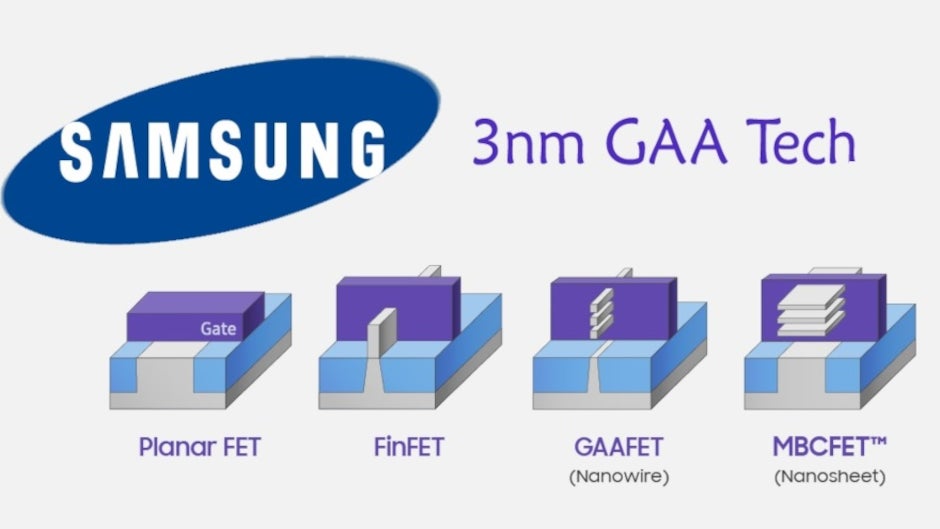
Samsung Foundry, the second largest independent foundry in the world after TSMC, has made some changes to its 3nm process node according to AnandTech. Samsung Foundry’s first chips to be produced using the 3nm, 3GAE (3nm Gate-All-Around Early) process, are said to be undergoing high volume manufacturing a year later than usual. It was also removed from Samsung’s roadmap, indicating that 3GAE could be produced for internal use only.
A representative from Samsung said: “Regarding the 3GAE process, we have been in discussion with customers and plan to mass-produce 3GAE in 2022.” The successor to 3GAE, the 3GAP (3nm Gate-All-Around Plus) node is still on the roadmap with volume manufacturing expected to begin in 2023. The aforementioned roadmap was unveiled at the Foundry Forum 2021 in China. Samsung Foundry presented its updated technology roadmap which was later reposted on Baidu and Weibo.
As for its chips using the older FinFET transistor architecture, Samsung has added 5LPP and 4LPP to its roadmap with high-volume manufacturing slated for 2021 and 2022, respectively. When Samsung unveiled its 3GAE and 3GAP nodes in May 2019, it announced that it will offer a 35% increase in performance, a 50% reduction in power consumption compared to 7LPP which is currently the process node of previous generation.

Samsung Foundry’s roadmap does not indicate high-volume production in 2022 for the 3GAE process node, likely an indication that it will be used for internal components
At the same time, in 2019, volume production using 3GAA (Gate-All-Around Transistor Architecture) was announced to start in late 2021. With the new launch date of 2022 for the Gate-All-Around Early 3 process. nm, it can be concluded that there was a slight delay on the part of Samsung or a miscalculation. Either way, this is not seen as a big deal as Sammy’s Early knots are not widely used by manufacturers.
Just a few days ago, Samsung Foundry registered a 3nm chip that uses its Gate-All-Around (GAA) transistor architecture. Registering a chip is the final act of its design cycle, resulting in one of two outcomes: the chip design works or not. In the latter case, a minor correction may be necessary or a complete design overhaul is required.
[ad_2]
Source link