
[ad_1]
The A16 Bionic could be the first chip built on the 3nm process node

Pple’s A14 Bionic chip was the first 5nm SoC used in a smartphone
If TSMC follows this roadmap, we should see the iPhone 14 line become the first Apple-made handsets to use chips produced with the 3nm process node. The first such chip would be the A16 Bionic. Last November, TSMC completed the structure of its 3nm plant at Southern Taiwan Science Park (STSP). TSMC originally planned to start 3nm test production at the end of 2020. But the global pandemic has forced TSMC to postpone this for a year.
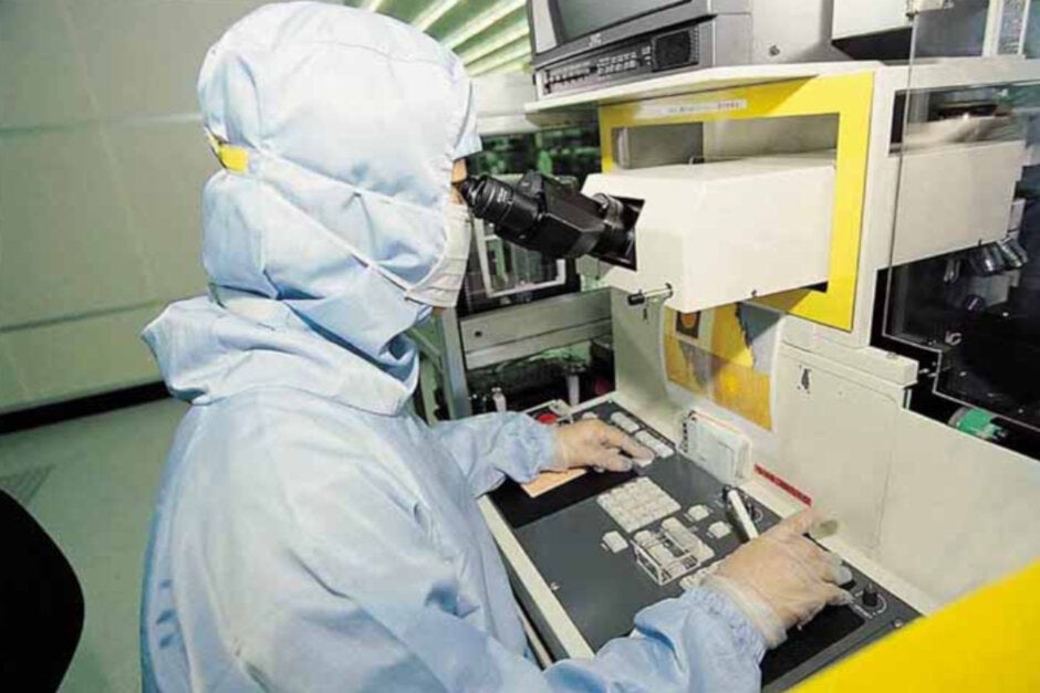
Instead of spending $ 20-28 billion this year on capital expenditures, analysts estimate, TSMC says that range will be higher, from $ 25 billion to $ 28 billion. The complexity of the technology required to build 3nm chips is one reason for the increased expense. TSMC also hemorrhages cash by purchasing EUV lithography equipment. Extreme ultraviolet lithography is used to engrave extremely fine lines on a wafer. These are the models that determine the locations of transistors inside a chip. Since billions of transistors are used in each chip, these lines need to be as thin as possible and this is where the EUV Litography machine comes in.
TSMC will use FinFET transistors for its 3nm chips while Samsung will switch from FinFET to GAA (gate-all-around). For 2nm, TSMC will use a GAA design. Samsung reportedly spent around $ 116 billion to develop its 3nm integrated circuits. We could see mass production of 2nm chips from 2024 at the earliest.
The observation made by Intel co-founder Gorgon Moore, known as Moore’s Law, called for the density of transistors to double every two years and in recent years we have not seen industry fully adhere to this law. And now, with 2nm within range, the question is whether Moore’s Law can continue. Foundries have been working on the use of alternative materials that can continue to improve chip performance and power consumption beyond 2nm. Just as EUV helped keep Moore’s Law valid after the 10nm process node, something new could be found to keep Moore’s Law alive.
[ad_2]
Source link