
[ad_1]
On the occasion of Intel's Investor Day, CEOs Bob Swan and Murthy Renduchintala spoke about the company's manufacturing capabilities. Intel has always been strong in its ability to execute its process technology, but the delay of its process to 10 nm has obviously raised many questions for several years. The two Intel executives explained in detail what Intel was doing in the meantime and how he learned from these issues.

In 2013, Intel planned to succeed the 10 nm technology by offering a density 2.7x, with new technologies such as SAQP (Self-Aligned Quad Patterning), COAG (Contact Over Active Gate), Cobolt interconnections and new technologies packaging such as EMIB and Foveros. Intel admits it was an ambitious plan and the goals were not clearly defined with the teams. It was ultimately too complex and not ideally managed.
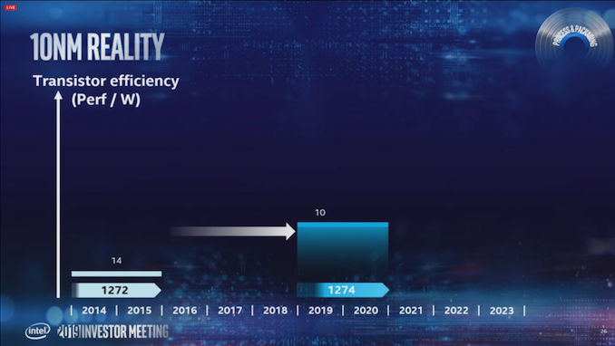
This ended up pushing 10 nm in a later period. In this case, Intel pushed 10 nm until 2019 (technically, they shipped Cannon Lake in small quantities on 10 nm in 2017, but this is nothing more than a curiosity in the semiconductor timeline) and filled the gap with 14+ and 14+. .
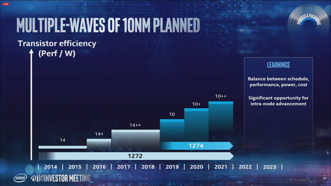
The Intels 14+ and 14 ++ processes have extracted over 20% more performance (from Broadwell to Whiskey Lake) of the process since its inception. As a result, Intel is ready not only to prepare for future intra-node optimizations, but also to adjust the roadmap to compensate for it. Murthy made it clear that Intel wanted to introduce a gain similar to that of Moore's Law at the beginning of a new process and another similar gain at the end of the process.
Intel has announced that its 10nm product family (beyond Cannon Lake) will be available from the middle of this year (2019), with Ice Lake on client platforms (laptops).

Intel will launch several 10nm products by 2019 and 2020, including the 10nm server-based first half of 2020:
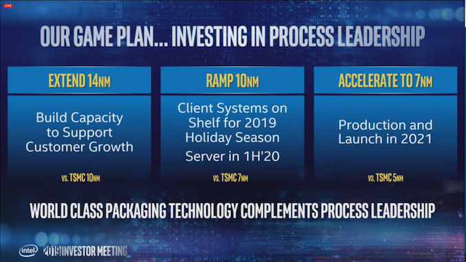
In the above slide, Intel states that it will produce 7 nm and will launch a product in 2021. This seems very aggressive for a company that has already had problems with 10 nm. This is seen even in Intels radels, 10nm (and 10+ and 10+) having a much shorter life cycle than the 14nm process family.
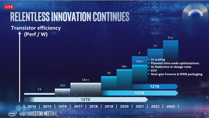
Keeping this in mind, the Intel 7nm will be the combination of what Intel has learned from the 14nm and 10nm family of products. Intel wants a 2x scaling (Moores law), but with intra-node optimizations planned as part of the roadmap. Intel also reduces its number of design rules, which should make it easier to run. 7nm will also be the meeting point between Intel and EUV, as well as the introduction of new generation Foveros and EMIB.
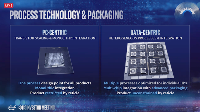
Intel provided this slide that shows a PC-centric monolithic chip with a data-centric multi-chip chip, built on both Foveros and EMIB. This corroborates our discussion with Intel's chip and packaging team, which also said we would see Foveros and EMIB on a combined product – specifically the GPU.

Intel has announced that its flagship product 7 nm (lead = top or lead = first?) Would be its new GPGPU, built on Xe graphics architecture. Intel said its stack of Xe products would feature two different microarchitectures ranging from mobile client to GPGPU, one of them calling Arctic Sound. Technically, Intel will launch its first discrete GPU in 2020 according to its press release, but the 7n GPNP will be launched in 2021.
More information come out of the Intel event, more to follow.
Related reading
Source: Intel
[ad_2]
Source link