
[ad_1]
With the development of carbon nanotubes and graphene, scientists have received a whole new collection of working materials: sheets and tubes that can be made with thicknesses equivalent to those of individual atoms. These materials promise to build electronic devices smaller than those currently possible by any other process and whose properties can be adjusted using different starting materials.
Until now, attention has focused on recreating new versions of familiar devices. But a new article written by a group of Shanghai researchers examines what can be done if you are not limited by the type of devices that we currently manufacture in silicon. The result is a device capable of performing basic logic in half the silicon needs of transistors, switch between different logical operations using light and store the output of the transistor. operation in the device itself.
OR or AND?
The computer instructions can be summarized in a series of simple logical operations. Among these theses, the simplest are AND and OR. AND produces a value of 1 only if its two entries are also 1; OR does it if one of the two entries is 1.
However, there is an imbalance between these logical operations and what we can do with silicon: a silicon transistor can take as input only one source instead of the two required here. Therefore, these operations require two transistors on a processor.
Transistors made of an extremely thin material can, however, have fundamentally different structures. The researchers used molybdenum disulfide (MoS) to test some of them.2), which forms graphene-type leaves slightly thicker than the atoms that compose it. Like silicon, moS2 is a semiconductor; unlike silicon, it is relatively easy to place input grids above and below a single layer of material. This allows the layer to input two different sources, making it a direct match with the logical operation input.
Better yet, the researchers discovered that they could create extremely similar devices performing different logical operations. MoS2The individual layers of can be atomically thin, but it is possible to stack several layers on top of each other. Initially, with only a few stacked leaves, the MoS2 formed a single semiconductor layer that would pass driving only if the doors above and below were in the "on" state. This corresponds perfectly to the AND function.
But keep adding layers, and the thickness would eventually reach a point where the top and bottom grids could independently control the conduction of MoS sheets.2 close to them. The authors compared it to two "channels" on the same device. If any of these channels were set to "on", a certain current would flow into the device, making its overall state "on". This was a perfect match with the logical OR function.
The critical thickness has proven to be four nanometers, less than half the size of the existing features in the state-of-the-art chips. If the MOH2 the sheets were stacked in a layer greater than 4 nm, the transistor would behave like an OR gate. Below this thickness, and it would perform AND operations.
Light and memory
At this point, the newspaper has moved on to something like "but wait, there is more!" One demonstration was that it is possible to turn an AND device into something that performs OR operations using the right wavelength of light. The essential of this is that the entrance gates work by exciting electrons in MoS2 in a state where they help to carry the current. In a thin layer of MoS2Both inputs must push electrons into the conduction band to circulate the current. This gives us an AND function.
But a light of appropriate wavelength can also push electrons into the conduction band. As a result, the light reduces the need to have conductive electrons induced by the input. As a result, it is sufficient for one of the two input gates to be in the "on" state for the transistor to be conducting. So, light on a thin sheet of MoS2 is enough to convert an AND device to an OR device.
The researchers did not stop there either. For their last demonstration, they slipped a layer of graphene next to the MoS.2. Graphene is able to capture and store some of the conductive electrons. If the transistor finds itself in the "on" state, enough of these electrons will spill over into the graphene that it will have a charge sufficient to keep it in the "on" state. And it is there that the transistor will remain until the electrons are specifically drained from graphene. In this way, graphene can act as a one-bit memory, storing the results of a past operation until the device is reset.
How many transistors do we really need?
Overall, the work is a good reminder that materials have atomically distinctive thin properties compared to the things we are currently working with, and it's worth thinking about how to take advantage of these properties in ways that effective. Halving the number of transistors needed for basic logic operations seems to be a good way to dramatically reduce the complexity of chips.
To some extent, the light-based switching shown here is contrary to what access from the transistor needs to be maintained for the pump light in it. Nevertheless, there are probably cases where optical circuits are embedded in a chip when it can be useful. Having a situation where the operating results can be stored in the transistor that performed the operation might be useful, but it would take a radically different programming model to do everything.
Because of these complications, it is unclear whether these specific demonstrations will bring much. But should MoS2 find your way in tokens for whatever reason you can expect people will look for ways to take full advantage of its capabilities.
Nature Nanotechnology, 2019. DOI: 10.1038 / s41565-019-0462-6 (About DOI).
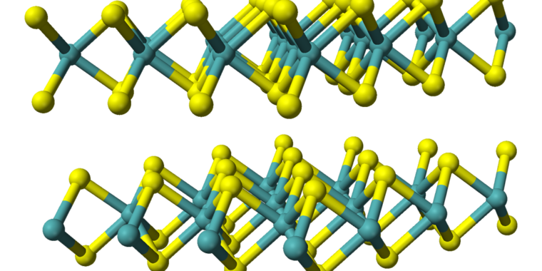
Image illustrated by the crystalline structure database of the American mineralogist
[ad_2]
Source link