
[ad_1]

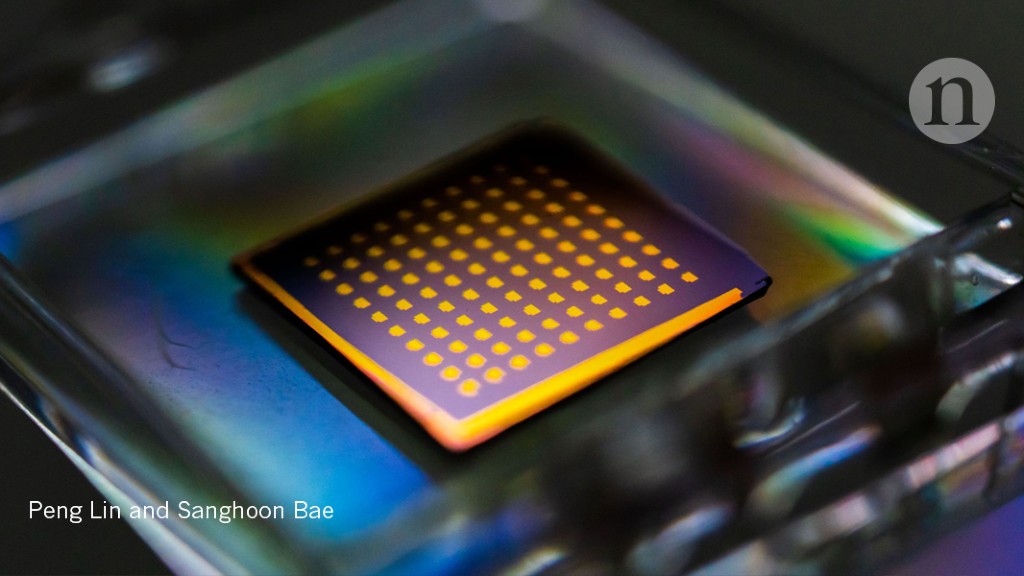
Chips made from stacks of single molecule transistors could power the next generation of computers.Credit: Peng Lin and Sanghoon Bae
The number of components in electronic circuits has doubled every two years since the 1960s – a trend known as Moore's Law. The transistors have been shrunk, so that more and more people can fit on a silicon chip. But now, silicon transistors are reaching their physical limit. Radically different types of hardware and equipment are needed to harness the potential of the next generation of computers.
The problem is common to all solid-state (3D) semiconductor based transistors, including those in germanium, indium gallium arsenide, and indium phosphide. Electrons have trouble traveling through channels of a nanometer thickness. Imperfections in the channel surfaces disperse the charges, slowing down their flow.
But 2D materials could allow transistors to continue to shrink. These are leaves of crystalline atoms, a thick layer. Because of their limited "vertical" dimension and their defect-free flat surfaces, the electrons are less prone to disperse and the charges can flow relatively freely through them. Promising materials include transition metal dichalcogenides (such as tungsten diselenide and molybdenum disulfide, MoS2).
However, this research is still in its infancy. For these materials to meet the needs of the industry for practical devices, three fundamental research problems must be solved.
Three challenges
Predict properties accurately. First, we need to find suitable materials for 2D transistors. There are over 1,000 applicants and their electronic properties vary enormously. It is faster to theoretically predict the electronic properties than to eliminate them experimentally, but it is difficult to accurately determine the behavior of a material in this way. Electron energies depend on the specific nature and disposition of atoms in the crystal lattice, which is often more complicated in real materials than in idealized models. The interactions between electrons and atoms must be taken into account, and approximations add uncertainty.
And experiments have shown that electrons are not as mobile as expected in 2D sheets. This is due to the scattering of electrons, but the processes involved are poorly understood. For example, how do the vibrations of the network slow down the electrons? Adjacent layers of materials, such as substrate and protective films, also have an influence, as do nearby fillers and imperfections. Physicists must take into account all these factors.
Grow and test samples. Promising candidates must be tested experimentally. It is important that the samples are of high quality and sufficiently large to fit into state-of-the-art transistors and simple reference circuits. Defects and grain boundaries affect the flow of charge1. Researchers must learn to cultivate uniform sheets of 2D materials with perfectly aligned crystals. They must also control the thickness of the layers to adjust the electronic properties.
There are two ways to make 2D sheets of crystals. The best option is to grow them by depositing vapor atoms in a vacuum chamber. They can also be formed by exfoliation, either by detaching the layers mechanically, or by putting them in solution. Peeling causes fewer network faults than loss, but the quantities produced are too small for practical devices.
During the formation of crystals, the substrate affects their growth. 3D materials bond closely to the underlying layer and follow its atomic geometries closely. In contrast, 2D materials are only weakly attached to the substrate, but are nevertheless influenced by it. For example, MoS2 Crystals grown on sapphire can follow two orientations (0 degrees and 60 degrees). Other materials form less oriented grains with similar boundaries to those of jigsaw joints. Some points end up having more than one molecular layer of thickness.
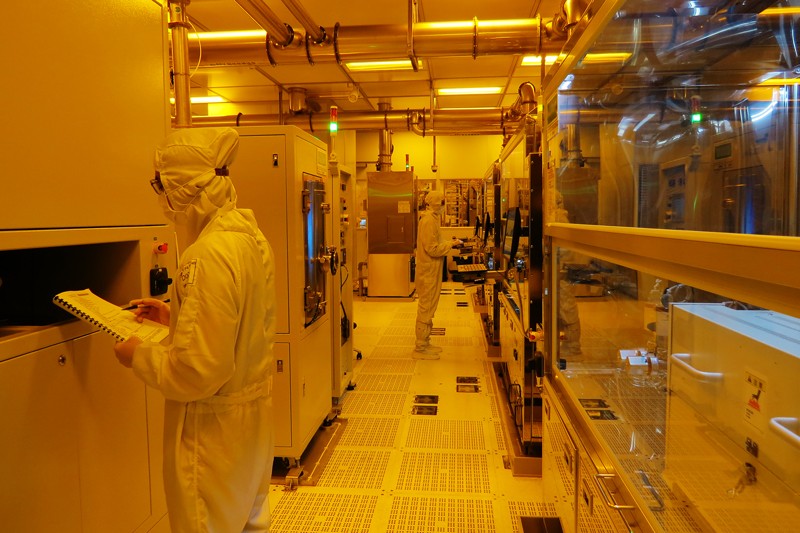
Researchers of the semiconductor materials research and advanced technology laboratory of the Taiwan Semiconductor Manufacturing Company in Hsinchu.Credit: Lain-Jong Li
2D materials must be chemically manufactured and thermally stable. For example, phosphorene and indium selenide degrade in ambient air in a few hours.2,3. The addition of a protective film, such as an oxide, can help preserve the material, but this adds another interface to take into account.
In the end, transistors must be reliably manufactured in large quantities. Today, the industry generally uses silicon substrates and silicon dioxide insulators, but these can not be used for oriented growth and their electrical quality can degrade at high temperatures (600 at 1000 ° C) necessary for the deposition of vapor atoms. Thus, 2D materials should be developed on expensive substrates of silicon carbide or sapphire, which can withstand such heat, and then transferred to silicon substrates for integration into the device. Molecular beam epitaxy (vacuum atom sputtering) is another method of growing 2D materials at lower temperatures (below 300 ° C), but it is slow: sample growth can take several days. Yield and reproducibility must also be improved.
Assessment of the performance of the device. The performance of different 2D materials must be evaluated in a common framework. Measurements reported in different contexts, or even in laboratories, may be inconsistent. The precise composition and structure of substrates, sandwich layers, electronic contacts and manufacturing processes are all important. And each type of device brings its own requirements. For example, a transistor in a logic switch must turn on and off abruptly, and an energy efficient transistor must operate at low voltage.
University and industry researchers should collaborate to develop measurement standards, similar to those defined for solar cell efficiency assessments by the US Renewable Energy Laboratory. These must specify, for example, the structure of the device, the metal contact criteria and the measurement procedures.
Collaboration and financing
The semiconductor chip industry, which accounts for nearly half a trillion dollars, should invest in solving these research problems; governments, idem. Graphene applications, the best-known 2D material, and its mass production methods are being developed as part of the European Commission's flagship research program, Graphene Flagship, with a budget of 1 billion euros (1.1 billion USD). But other 2D materials are still largely in the academic phase.
2D materials should play a bigger role in electronic programs exploring materials for logic, memory and connections. One of these efforts is the 2D atomic layer research and engineering program of the US National Science Foundation. Several groups, such as Semiconductor Research Corporation, a non-profit consortium based in Durham, North Carolina, are expected to put in place programs to accelerate the development of 2D materials.
It is too early to say whether 2D semiconductors will transform transistors. But they are one of the best candidates to extend Moore's law.
[ad_2]
Source link