
[ad_1]
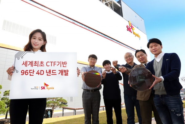
NAND TAND 4D NAND 512 Gbit 96-level TLC with the highest efficiency on the market
The SK Hynix 4D NAND SK is characterized by the combination of the CTF cellular structure and PUC technology that most companies, including SK Hynix, use in 3D NAND, unlike the combination of PUC and the cellular structure with floating door. SK Hynix has named this product "CTF-based NAND 4D Flash" to highlight the difference between implementing the best performance and productivity of the market by introducing for the first time the PUC into CTF based on excellent features. .
CTF technology is a technology that innovatively eliminates performance and productivity by minimizing inter-cell interference. Currently, most large NAND flash companies, including national companies, are currently recruiting floating gates primarily used in existing 2D NANDs. The PUC technique is a technique for placing an underlying peripheral circuit in the operation of a cell under a cell region storing data. This can be compared to the optimization of space by transforming the outdoor parking of an apartment into an underground car park.
The chip size was reduced by more than 30% and the number of bits per slice was multiplied by 1.5 compared to the 72-level 512 Gbit 3D NAND. In addition, four plans are placed in a chip, doubling the data bandwidth (data bandwidth) to 64 kilobytes, the highest level in the industry.
In addition, it is developed to be mounted on a smartphone mobile package using the small size of the chip that is the advantage of 4D NAND compared to the existing 3D NAND. For example, SK Hynix's five-stage, NAND 4D NAND 4D can completely replace two existing 256 Gbit 3D NANDs, which is very cost-effective. This innovation has increased the writing and reading performance of this product by 30% and 25%, respectively, compared to the existing product in 72 steps.
In addition, by adopting a multi-door insulating structure and new design technology, the data transfer rate per input / output (information in / out) is increased to 1,200 Mbps and the operating voltage is reduced to 1, 2 V (volt). .
SK Hynix said during a speech at the Flash Memory Summit (FMS) held in Santa Clara (USA) in August that he will be launching his next-generation NAND 4D NAND flash solution and will strengthen its responsiveness on the market. FMS is the world's largest forum for the NAND flash industry with over 5,000 participants.
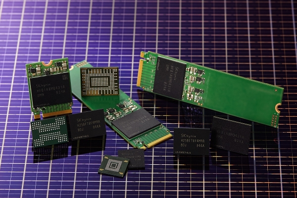
First, it is planned to display a SSD drive up to 1 TB (client) with up to 512 TB 4 NAND 4D with its own controller and firmware.
The 72-step SSD, which has already been certified by major customers such as Hewlett-Packard and Microsoft, as announced by the existing FMS, is expected to grow to 96 steps next year, boosting the business and competitiveness of SSDs. .
UFS (Universal Flash Storage) 3.0, which is expected to be adopted in next generation smartphones, will be launched in the first half of next year with its own controller and firmware. This product is also comprised of 96-level, 4D 512Gbit 4D NAND cards and is expected to contribute to the future capacity and performance of mobile devices, including 5G, with remarkably improved performance and energy efficiency. significantly improved compared to the current 256 Gbit NAND products on the market.
SK Hynix plans to commercialize Tbit 1 Tbit (TeraBit) and QLC (Quad Level Cell) 1 Tbit products based on 96-stage NAND 4D.
According to the TrendFocus market research, SK Hynix's SSD market share (in quantity) increased from 5.6 percent in the second quarter of last year to 9.9 percent in the second quarter of this year. In particular, with the launch of enterprise SSDs starting in the third quarter of this year, SK Hynix's SSDs market share is expected to increase steadily, as will the new 96-stage NAND 4D, which should enhance the competitiveness of solutions, especially enterprise SSD drives.
Kim Jung-tae, SK Hynix's NAND Marketing Manager, said, "The FCT-based 4D 96-story product, which will be a future development platform, will be a milestone for SK Hynix's NAND flash market. , which offers the industry's highest competitiveness and performance.We will begin mbad production of the recently completed M15, and actively respond to customer requests. "
Copyright © © HaitianBiz, reprinting and redistribution prohibited
Source link
