
[ad_1]

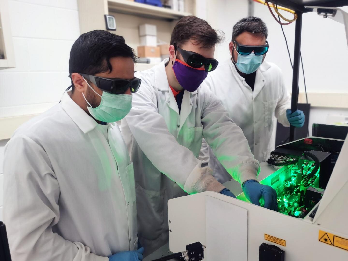
From left to right, Pan Adhikari, Lawrence Coleman, and Kanishka Kobbekaduwa line up the ultra-fast laser in the UPQD laboratory of the Department of Physics and Astronomy. Credit: Clemson University
By using laser spectroscopy in a photophysics experiment, researchers at Clemson University have broken new ground that could result in faster, cheaper energy to power electronics.
This new approach, using perovskite treated in solution, aims to revolutionize a variety of everyday objects such as solar cells, LEDs, photodetectors for smartphones and computer chips. Solution-treated perovskite is the next generation material for rooftop solar cell panels, x-ray detectors for medical diagnostics, and LEDs for everyday lighting.
The research team included a pair of graduate students and an undergraduate student mentored by Jianbo Gao, group leader of the Ultrafast Photophysics of Quantum Devices (UPQD) group in the Department of Physics and Astronomy at the College of Science.
The collaborative research was published on March 12 in the high-impact journal Communications of nature. The article is entitled “In situ observation of trapped supports in organic metal halide perovskite films with ultra-fast temporal and ultra-energetic resolutions”.
The principal investigator was Gao, who is an assistant professor of condensed matter physics. Co-authors included graduate students Kanishka Kobbekaduwa (first author) and Pan Adhikari from the UPQD group, as well as Lawrence Coleman, a senior in the physics department.
Other Clemson authors were Apparao Rao, RA Bowen physics professor, and Exian Liu, a visiting student from China who works under Gao’s guidance.
“Perovskite materials are designed for optical applications such as solar cells and LEDs,” said Kobbekaduwa, graduate student and first author of the research paper. “This is important because it is much easier to synthesize compared to current silicon based solar cells. It can be done by solution processing – whereas in silicon you have to have different methods which are more expensive and more expensive. long. “
The goal of research is to make materials that are more efficient, cheaper and easier to produce.
The unique method used by Gao’s team – using ultra-fast photocurrent spectroscopy – allowed much higher temporal resolution than most methods, in order to define the physics of trapped carriers. Here, the effort is measured in picoseconds, or one trillionth of a second.
“We make devices using this material (perovskite) and we use a laser to shine light on them and excite the electrons inside the material,” Kobbekaduwa said. “And then using an external electric field, we generate a photocurrent. By measuring this photocurrent, we can effectively tell people the characteristics of this material. In our case, we have defined the trapped states, which are defects in the material that will affect the current we get. “
Once the physics are defined, researchers can identify flaws – which ultimately create inefficiency in materials. When faults are reduced or passivated, it can lead to increased efficiency, which is essential for solar cells and other devices.
As materials are created by solution processes such as spin coating or inkjet printing, the likelihood of introducing defects increases. These low temperature processes are less expensive than the very high temperature processes which result in pure material. But the compromise is more flaws in the material. Finding a balance between the two techniques can mean better and more efficient devices at a lower cost.
The substrate samples were tested by shooting a laser at the material to determine how the signal propagates through it. The use of a laser to illuminate the samples and collect current made the work possible and differentiated it from other experiments that did not employ the use of an electric field.
“By analyzing this current, we can see how the electrons move and how they come out of a fault,” said Adhikari of the UPQD group. “This is only possible because our technique involves ultra-fast timescale and in situ devices under an electric field. Once the electron falls into the fault, those who experiment using other techniques don’t can not remove it. But we can remove it because we have the electric field. Electrons have a charge under the electric field, and they can move from one place to another. We are able to analyze their transport from point to point within the material. “
This transport and the effect of material defects on it can impact the performance of these materials and the devices in which they are used. It’s all part of the important discoveries students make under the guidance of their mentor, creating ripples that will lead to the next big breakthrough.
“Students don’t just learn, they actually do the work,” Gao said. “I am fortunate to have talented students who, when inspired by challenges and ideas, will grow into influential researchers. This is all part of the important discoveries students make under the guidance of their mentors, creating ripples that will lead to the next big one.We are also very grateful for the strong collaborations with Shreetu Shrestha and Wanyi Nie, who are the best materials scientists. from Los Alamos National Laboratory. ”
New study reveals secrets of solar success
Kanishka Kobbekaduwa et al, In-situ observation of carriers trapped in organic metal halide perovskite films with ultra-fast time and energy resolutions, Nature communications (2021). DOI: 10.1038 / s41467-021-21946-2
Provided by Clemson University
Quote: Researchers Breakthrough in Solar Cell Materials (2021, March 12) retrieved March 12, 2021 from https://phys.org/news/2021-03-breakthrough-solar-cell-materials.html
This document is subject to copyright. Other than fair use for private study or research purposes, no part may be reproduced without written permission. The content is provided for information only.
[ad_2]
Source link