
[ad_1]

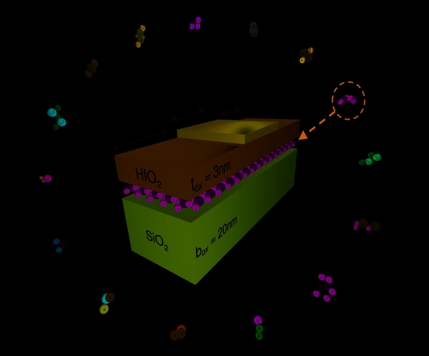
Around it, a selection of 2D materials that have been studied. Credit: Mathieu Luisier / ETH Zurich
With the increasing miniaturization of electronic components, researchers are grappling with unwanted side effects: In the case of nanoscale transistors made of conventional materials such as silicon, quantum effects occur that alter their functionality. One of these quantum effects, for example, is additional leakage currents, that is, currents that flow “stray” and not through the intended conductor between the source and drain contacts. It is therefore believed that Moore’s scale law, which states that the number of integrated circuits per unit area doubles every 12 to 18 months, will reach its limits in the near future due to the increasing challenges associated with the miniaturization of their. active components. This ultimately means that the currently manufactured silicon-based transistors – called FinFETs and found in almost all supercomputers – can no longer be made arbitrarily smaller due to quantum effects.
Two-dimensional beacons of hope
However, a new study by researchers at ETH Zurich and EPF Lausanne shows that this problem could be overcome with new two-dimensional (2-D) materials – or at least that’s what the simulations are. they carried out on the “Piz Daint” supercomputer suggest.
The research group, led by Mathieu Luisier from the Institute for Integrated Systems (IIS) at ETH Zurich and Nicola Marzari from EPF Lausanne, used the research results that Marzari and his team had already obtained as the basis for their new simulations: Back in 2018, 14 years after the discovery of graphene for the first time, it was clear that two-dimensional materials could be produced, they used complex simulations on “Piz Daint” to sift through a pool of more than 100,000 materials; they extracted 1,825 promising components from which layers of 2D material could be obtained.
The researchers selected 100 candidates from these more than 1,800 materials, each of which consists of a single layer of atoms and could be suitable for the construction of ultra-scale field effect transistors (FETs). They have now studied their properties under an “ab initio” microscope. In other words, they used the CSCS “Piz Daint” supercomputer to first determine the atomic structure of these materials using Density Functional Theory (DFT). They then combined these calculations with a so-called Quantum Transport solver to simulate the flow of electrons and holes through the virtually generated transistors. The quantum transport simulator used was developed by Luisier with another research team from ETH, and the underlying method received the Gordon Bell Prize in 2019.
Find the optimal 2D candidate
The decisive factor for the viability of the transistor is whether the current can be optimally controlled by one or more gate contact (s). Thanks to the ultra-thin nature of 2D materials – typically thinner than a nanometer – a single gate contact can modulate electron flow and hole currents, thereby completely switching a transistor on and off.
Structure of a single gate FET with a 2D material channel. Around it, a selection of 2D materials that have been studied. (Mathieu Luisier / ETH Zürich)
“Although all 2D materials have this property, not all of them lend themselves to logic applications,” emphasizes Luisier, “only those which have a sufficiently large band gap between the valence band and the conduction band.” Materials with an appropriate bandgap prevent so-called electron tunneling effects and therefore the leakage currents they cause. It is precisely these materials that the researchers were looking for in their simulations.
Their goal was to find 2D materials capable of delivering a current greater than 3 milliamps per micrometer, both as n-type transistors (electron transport) and as p-type transistors (hole transport), and whose channel length can be as small. like 5 nanometers without adversely affecting the switching behavior. “It is only when these conditions are met that transistors based on two-dimensional materials can outperform conventional Si FinFETs,” says Luisier.
The ball is now in the experimental researchers’ court
Taking these aspects into account, the researchers identified 13 possible 2D materials with which future transistors could be constructed and which could also allow the pursuit of Moore’s scaling law. Some of these materials are already known, for example black phosphorus or HfS2, but Luisier points out that others are completely new – compounds such as Ag2N6 or O6Sb4.
“We have created one of the largest databases of transistor materials through our simulations. With these results, we hope to motivate experimenters working with 2D materials to exfoliate new crystals and create next-generation logic switches ”, explains the ETH professor. The research groups led by Luisier and Marzari work closely together at the National Center of Research Skills (NCCR) MARVEL and have now published their latest joint findings in the journal ACS Nano. They are convinced that transistors based on these new materials could replace those made of silicon or the currently popular transition metal dichalcogenides.
Simulation microscope examines transistors of the future
Cedric Klinkert et al, 2D materials for ultrascale field effect transistors: one hundred candidates under the Ab Initio microscope, ACS Nano (2020). DOI: 10.1021 / acsnano.0c02983
Provided by the National Center for Research Skills (NCCR) MARVEL
Quote: Two-dimensional Materials for Ultrascaled Field Effect Transistors (August 17, 2020) retrieved August 19, 2020 from https://phys.org/news/2020-08-two-dimensional-materials-ultrascaled-field-effect-transistors. html
This document is subject to copyright. Other than fair use for private study or research purposes, no part may be reproduced without written permission. The content is provided for information only.
[ad_2]
Source link