[ad_1]
AMD announced today its product development plans for the coming years, offering a range of new processors and new graphics processors.
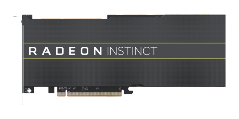
On the front of the GPU, two new data center-oriented GPUs: the Radeon Instinct MI60 and MI50. Based on Vega architecture and based on TSMC's 7 nm process, the cards do not primarily target graphics (despite what one might think since they're calling for GPU), but rather the applications of machine learning, high performance computing and rendering.
The MI60 will have 32 GB of ECC HBM2 memory (second generation bandwidth memory), while the 16 GB MI50 will have a memory bandwidth of up to 1 TB / s. ECC is also used to protect all the internal memory of the GPUs themselves. The cards will also support PCIe 4.0 (which doubles the transfer rate of PCIe 3.0) and GPU-to-GPU direct links using the Infinity Fabric software from AMD. This will provide up to 200 GB / s of bandwidth (three times more than PCIe 4) between up to 4 GPUs.
The cards will support a wide range of data types for calculation; for neural networks and machine learning, there is 16-bit floating point support at half precision and 4-bit and 8-bit full support; for HPC workloads, there is a simple (32-bit) and double (64-bit) precision floating point. AMD says the MI60 will be the fastest double-precision accelerator, with a capacity of up to 7.4 T / F, while the MI50 will not be far behind with a TAN 6.7.
The cards also include built-in support for virtualization, allowing a card to be shared securely between multiple virtual machines. Cloud operators thus more easily offer virtual machines accelerated by a graphics processor.
The MI60 will be shipped to customers of the data center by the end of the year. The MI50 arrives a little later but should be available by the end of the first quarter of 2019.
On the processor side, AMD talked a lot about future Zen architecture. The goal of the original Zen architecture was to allow AMD to be at least competitive with what Intel had to offer. AMD knew that Zen would not accept Intel 's performance, but the pricing and features of its chips made them nonetheless attractive, especially for workloads highlighting some component shortcomings. Intel (fewer memory channels, less I / O bandwidth). Zen 2 promises to be not only competitive with Intel, but superior to him.
AMD
The 7 nm process of TSMC, which offers a transistor density twice that of the 14 nm process, is one of the key elements of this evolution. For the same level of performance, the power is reduced by about 50% or, conversely, at the same power consumption, the performance is increased by about 25%. TSMC's 14 nm and 12 nm processes lag behind the Intel 14 nm process in terms of performance per watt, but with 7 nm, TSMC will take the lead.
Zen 2 will also address some weak aspects of the original Zen. For example, the original Zen used 128-bit data paths to handle 256-bit AVX2 operations; each operation was split into two parts and processed sequentially. In workloads using AVX2, this, with its native 256-bit implementation, was a huge advantage for Intel. Zen 2 doubles floating-point and 256-bit data paths, doubling the available bandwidth and dramatically improving the performance of this code. For entire workloads, branch prediction and prefetching have been made more accurate and some caches have been expanded.
Zen 2 will also offer improved hardware protection against some variants of Spectrum attacks.
The original Zen used a multi-chip module design. The chips used one, two, or four arrays (for Ryzen, respectively first-generation Threadripper and second-generation Epyc / Threadripper), all in a single package. Each chip contained two main complexes (four-core blocks), two memory controllers, Infinity Fabric links (for connections between arrays), and PCIe channels. This allowed AMD to switch from Ryzen to a single chip, 8-core / 16-wire at the 32-core / 64-wire Epyc.
The original Zen topology: Each matrix contains all the parts needed for a complete processor.
AMD
Zen 2 takes a very different approach, even if it still uses a multi-chip design. Instead of each chip containing CPUs, memory controllers, and I / O, the new design divides the different roles. There will be a single 14nm I / O chip, with 8 memory controllers, 8 Infinity Fabric ports and PCIe lines, then a number of 7nm "chiplets" containing only processors and Infinity Fabric. This new approach should remedy some of the most delicate aspects of the original zen; for example, there is a significant latency overhead when a kernel on a Zen dice must use the memory of another dice. With the Zen 2 design, the latency of memory should become much more uniform.
The new Zen 2 design: common I / O functions are placed on the 14-nm I / O chip, with the 7-nm "chiplets" containing only CPUs.
AMD
According to AMD, Zen 2 is currently sampling, with processors expected to hit the market in 2019. Zen 3, using an improved 7nm process, is currently "on track" and is expected to land in 2020, and Zen 4, on a more advanced process, is currently in the design phase.
Source link
