[ad_1]
Before the annual Supercomputing 2018 conference next week, Intel announces today a portion of its upcoming strategy for Cascade Lake. In the wake of its scalable Xeon Scalable Skylake family of servers, Intel has already announced that Cascade Lake-SP will be the next generation, computing and security-oriented. Today's announcement is the opening of a family of products alongside Cascade Lake-SP, called Cascade Lake-AP or Cascade-AP. Cascade-AP will aim for "advanced performance". In order to implement this new family of processors, Intel combines several chips in the same package.
Scaling up to 48 cores per processor
Intel is still keeping a lot of details about Cascade-AP, but we know some high-level specifications: Cascade-AP processors will have up to 48 cores, possibly with hyperthreading, and are intended for dual-socket servers. , for a total of 96 cores in a 2S system. As a result, a single Cascade-AP is essentially a 2S Xeon configuration on a single chip.
Each Cascade-AP processor will have 12 DRAM DDR4 channels, although maximum memory capacity has not been announced. The connection between the processors corresponds to the standard UPI connection, as seen on the current Xeon Scalable processors, although the connection speed has not been specified. It seems that Cascade-AP is not designed to evolve beyond a 2S system.
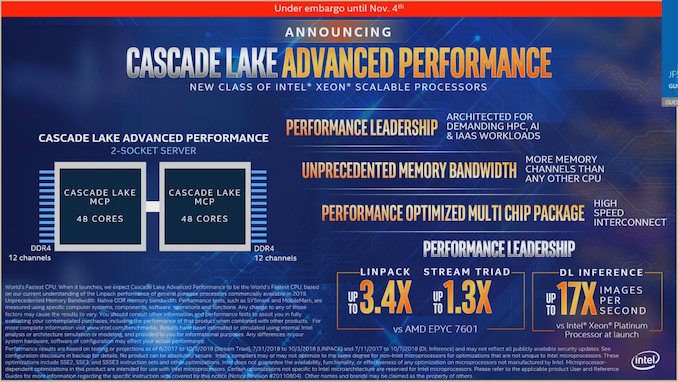
Each Cascade-AP lake processor will offer up to 48 cores and to do this, Intel uses a multi-chip package (MCP). At this point, we believe that Intel is using two silicon chips in the package, specifically two "XCC" chips that should be designed with 28 cores but will only activate up to 24 cores per silicon. Intel has confirmed that these matrices are connected by UPI on the package and not with Intel's EMIB technology. It's a shame, considering how Intel has promoted its EMIB technology as an alternative to the interposer, but we have not seen it yet in a product that connects two high-power chips, as expected at the time. origin at the announcement of the technology. This means, however, that it can use the same silicon that is found in standard Xeon Scalable processors.
No information was provided on the TDP per processor, nor on pricing, PCIe channels, memory capacity / storage, frequencies or variants. We were told that it would be launched at the same time as the entire Cascade Lake family, "in the first part of 2019" (to quote directly). Intel gave some basic performance figures, suggesting that a processor gets scores 3.4 times higher than those of an EPYC 7601 under Linpack and 1.3 times higher under Stream Triad. Deep Learning inference, a major workload for these new parts, has been cited as giving Skylake-SP's core launch performance 17 times, which is 1.55 times the launch performance of Cascade-SP cited in the origin with the new VNNI instructions.
Given the additional energy and memory requirements, we expect Intel to use a new socket for this processor. Rather than LGA4367, with 4367 pins, there have been recent leaks suggesting that a LGA5903 socket is where Cascade-AP will end, although Intel has not confirmed it. As part of its advance access program, Cascade-AP will release revenue for the third quarter of 2018 to its distinguished customers. However, their availability will be extended "in the first part of 2019".
More cores per socket, but potentially a worse 4S system
With this new type of processor, even with Intel's previous competitive analysis of MCP designs, Intel is increasing the number of cores per socket and cores per 2S system more and more. The 2S server market is one of the largest of Intel's in the entire company. The idea is to offer more value. It's hard to pinpoint the impact that Cascade-AP will have on the product portfolio, but let's not forget that Intel is trying to condense a 4P system into a 2P system, even though it will probably not work as well.
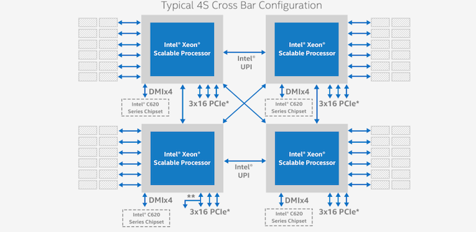
Take, for example, a 4P 24-core system with 96 cores in total. Thanks to Intel's 3 UPI links, communication between the four processors allows each processor to communicate with each other in a single hop. Each processor has six memory channels, access to 48 PCIe channels, potential access to OmniPath, and more.
In a Cascade-AP two-socket system, it all depends on how the links between the sockets are formed.
We already know that in the same package, the two silicon matrices will speak via UPI via the package. This power consumption is lower than that of a socket-to-socket UPI connection and can also take advantage of lower latency. All this is good and good.
But between the sockets are the questions. If Intel uses only one UPI link between sockets, only one chip in each socket will be connected. This is essentially a direct chain connectivity, which means that to talk to a silicon chip of the other socket, it sometimes takes two jumps.
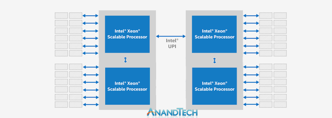
If Intel uses two UPI links between sockets, the situation is similar to that of a Xeon Gold-2UPI system where the processors are arranged in a square and there is no cross connection. This creates a communication imbalance between the processors and the memory, difficult to predict unless the software can enumerate and manage it effectively.
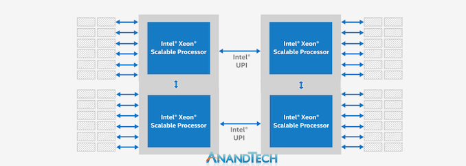
The other option is if Intel uses four UPI links between sockets – two of each silicon chip, to one of the other silicon chips on the other processor. This is identical to a 3UPI 4P system, with the difference that the double-tap configuration makes it all the more complex. It would take at least two UPI links to cross with the traces on the motherboard. This requires either a thick motherboard (which increases costs) or a control repeater chip that is easier to use. But even in this case, we are dealing with a non-uniform memory architecture in each socket and between sockets with different latencies between jumps. At least in a natural 4S system, the arrangement can guarantee that the latencies are equal.
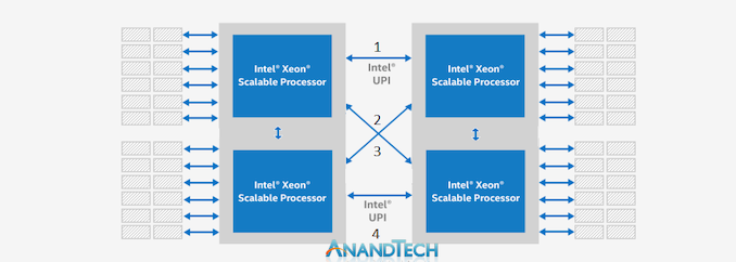
There is also the question of PCIe channels. Intel has not given any number, but we suspect that it is between 48 (24 by dice) and 96 (48 by dice) per socket. Which would be identical to a 4S system again.
In addition, a question of frequencies. The 24-core Xeon Platinum runs at 205W. Intel will not put the TDP at 410W when it will put two together – it will have to drop the frequency to hit something more suitable for the big socket. Add to that the complexity of providing 48 cores with enough power to be competitive. With separate chips, each socket can have higher frequencies.
The only positive point would be the actual physical volume. Some data centers deal only with compute density, and for some vendors looking to deploy many x86 processors in their offering, this solution could be a winner. Intel has repeatedly cited this Xeon-based inference as a major source of customers, hence the inclusion of features such as VNNI on Cascade Lake to help stimulate this market.
Chronology for Cascade Lake and Cascade Lake-AP
Intel said it was sending processors to generate revenue for some customers as part of its early adoption program. The new plays will be launched in the first part of 2019, with the Cascade Lake family (SP and AP) being launched simultaneously. We asked a series of relevant questions after our presentation, but Intel is not willing to respond to anything more than our presentation. Some additional information (or demonstrations) could be seen at the 2018 Supercomputing Conference to be held next week.
Source link
