
[ad_1]
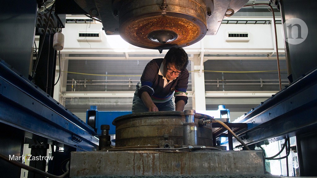
Takashi Taniguchi infiltrates one of the most powerful hydraulic presses in the world. This seven meter high machine can compress carbon into diamonds – but they are not on the menu these days. Taniguchi and his colleague Kenji Watanabe use it to cultivate some of the most sought-after jewels in the world of physics.
Over the past eight days, two steel anvils have ground a powdery mixture of compounds inside the press at temperatures above 1500 ° C and up to 40,000 times atmospheric pressure. Now, Taniguchi has opened the machine and the cooling water is flowing from his entrails. He catches the dripping price, a cylinder 7 centimeters wide, and starts shredding its outer layers with a knife to get rid of metal waste that has helped regulate pressures and temperatures. "The last steps are like cooking," he says, focusing on his tools. Eventually, it reveals a molybdenum capsule no bigger than a thimble. He puts it in a vise and grasps it with a wrench the size of his forearm. In a jiffy, the capsule breaks and releases a burst of excess powder in the air. Clear and clear crystals of millimeter size, also called hexagonal boron nitride (hBN), are always embedded in the capsule.
Materials Laboratories around the world want what Taniguchi and Watanabe are doing here at the Extreme Technology Lab, a building located on the leafy campus of the National Institute of Materials Science (NIMS) in Tsukuba, near Tokyo. Over the past decade, the two Japanese have been the world's leading creators and suppliers of ultra-pure hBN, which they have made available to hundreds of research groups at no charge.
They sacrificed much of their own research and almost all the time their press devoted to this task. But in doing so, they have accelerated one of the most exciting areas of research in materials science: the study of electronic behavior in 2D materials such as graphene, carbon sheets and other materials. an atom of thickness. These systems are exciting physicists who have fundamental knowledge of some of the most exotic electronic effects of the quantum world and could someday lead to applications in quantum computation and superconductivity – a conduct conducted without resistance.
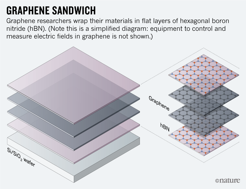
It is easy to make graphene itself by using tape to peel carbon layers from pencil lead (graphite). However, in order to study the complex electronic properties of this material, researchers must place it on an exceptional surface: a perfectly flat protective medium that will not interfere with fast-moving graphene electrons. This is where hBN is presented as an underlayer or a transparent substrate. "According to our research, this is the ideal substrate for hosting graphene or other 2D devices," says Cory Dean, a condensed-matter physicist at Columbia University in New York, a member of the team that worked for the first time. how to couple hBN and graphene. "It just protects the graphene from the environment in a beautiful way."
When an hBN flake comes in contact with graphene, it can also act as an adhesive film, allowing the carbon sheet to be accurately drawn and repositioned down. This allows researchers to create devices by stacking multiple layers of 2D materials, such as a sandwich (see 'Graphene Sandwich').
Since last year, for example, material scientists have been surprised by the discovery that it is enough to misalign two sheets of graphene by exactly 1.1 ° – a "magic angle" – the material can become a superconductor at very low temperature1,2. And in July, researchers reported signs of superconductivity when three sheets of graphene are stacked on top of each other – no twisting necessary3. These research studies, like hundreds of others, all used Taniguchi fragments and Watanabe hBN to protect their samples. "We are just involved," said Taniguchi modestly. "It's kind of a by-product for us." Dean is more eloquent about the hBN of the pair: "This is really the unsung hero of the process," he says. "It's everywhere."
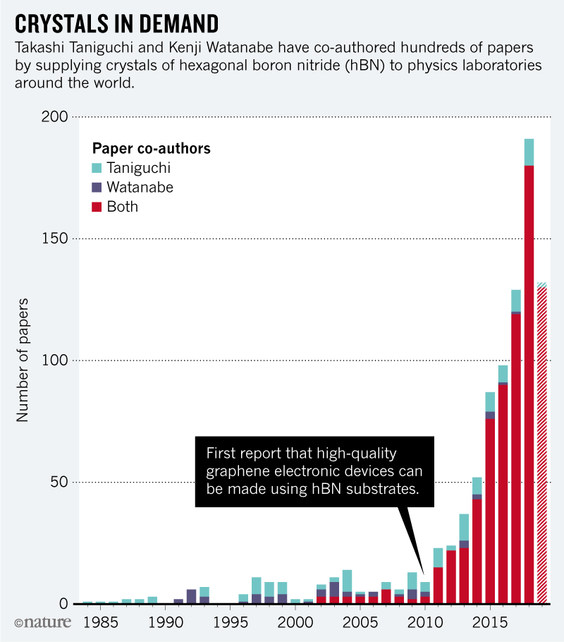
Neither Taniguchi nor Watanabe are graphene researchers and they did not know that their gems would become so desirable. Researchers now have several patents related to their process of making hBN, but say they do not expect to market it – for now, only research groups need the highest purity crystals. There is however a considerable advantage. Because they are the authors of studies on the use of their crystals, they are now among the most published researchers in the world. Taniguchi and Watanabe collaborated together on 180 articles last year. Since 2011, they have co-authored 52 articles in Science and Naturewhich makes them the most prolific researchers of these journals in the last 8 years (see "Crystals in Demand").
Source: Scopus /Nature
Their crystalline empire might not last forever: Taniguchi is about to retire, and other research groups are trying to create a high-quality hBN, which could help improve the supply and the speed up the search. But for the moment, physicists are somewhat reluctant to test untested samples when they know that they work so well, says Philip Kim, physicist of condensed matter at Harvard University in Cambridge, Massachusetts. . "Why Watanabe and Taniguchi? Because their crystal is the best. "
Under pressure
The impressive hydraulic press lives in a gigantic industrial space in Tsukuba's laboratory, filled with a continuous buzz of machines and light from tall windows, throwing dust rays on equipment below. The machine was built between 1982 and 1984, when the laboratory was part of the National Institute for Inorganic Materials Research (NIRIM), a precursor of NIMS. Taniguchi arrived five years later, after leaving a postdoctoral position at the Tokyo Institute of Technology. The press was originally designed to make diamonds, but in the 1990s, the Japanese government embarked on a research program called "Beyond Diamond" to find the next big novelty in ultra-hard materials, potentially to cut substances or for use in semiconductors.
One of the main candidates for the program was boron nitride in its cubic crystalline form (cBN), a dense structure in which the boron and nitrogen atoms are arranged like the carbon atoms of the diamond. Taniguchi first focused on growing ultra-pure cBN in the press – but his group was unable to remove impurities, lost carbon and oxygen particles that penetrated during sample preparation. The crystals thus appeared with an undesired dull brownish cast iron. . As a by-product, however, the process produced a clear hBN, in which hexagonally arranged layers of atoms slide easily over each other, in the same way as the carbon layers in the graphite .
Watanabe, a materials scientist and spectroscopist, joined NIRIM in 1994, just when the Beyond Diamond program was launched. He spent a few years studying the optical properties of diamonds. In 2001, while attempting interdisciplinary collaboration across the institute, Taniguchi knocked on Watanabe's door and invited him to take a look at his cBN crystals.
Both researchers have contrasting styles. Taniguchi is known for his parties, sweeps Queen's music in the lab while he runs the press late into the night and, even at the age of 60, still plays football with his colleagues at the club. Lunch time. Watanabe, three years younger, has a soft voice, is detail-oriented and prefers tennis. But the scientists worked well together and published their first article4 on cBN crystals in 2002.
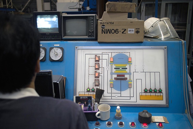
Taniguchi at the controls of his hydraulic press – with the CD Queen that he plays in the lab.Credit: Mark Zastrow
A year later, Watanabe, complaining about the quality of the cBN that Taniguchi passed on to him, glanced at a box of junk in the press. The crystals of hBN attract his attention and he decided to examine their properties. Taniguchi was skeptical: "I said:" It's hBN, which is boring! "". Watanabe, however, discovered something new: luminescent hBN under ultraviolet light, unlike diamond or cBN that he had been looking for for years. "It was the most exciting moment of my career," he says, a discovery that left him buzzing for weeks. The pair reported this result in May 2004, suggesting that hBN could be a promising crystal for UV lasers5.
Later that year, a pre-print of physicist Andre Geim and his team from the University of Manchester, UK, began circulating.6. They had succeeded in isolating single-atom graphene layers, launching craze for ultra-thin 2D materials. The frenzy of activity was something that Taniguchi and Watanabe observed with curiosity. "We had no idea about 2D materials," says Taniguchi. But, half a decade later, researchers in 2D materials were going to learn more.
A dazzling discovery
In 2009, the field of graphene had a problem. In theory, the material was remarkable, but researchers were struggling to exploit its full potential. The problem seemed to be that graphene, a single atom of thickness, marries the shape of the surface on which it is placed. The flatness that makes the material unique is lost if this substrate is not equally flat. Moreover, since graphene is so thin, the electrons passing through it are essentially in contact with the substrate on which it rests. This means that the substrate must be incredibly pure: any impurity will cause the dispersion of the electrons, thus reducing their mobility. Standard silicon oxide substrates were not good enough and seemed to limit the performance of graphene.
James Hone, mechanical engineer at Columbia University, and his post-doc, Cory Dean, had in mind a better substrate: hBN. It is atomically flat and has a wide band gap, which is an important energy barrier that prevents electrons bound to atoms from jumping into a conductive and mobile state. This makes hBN a good insulator.
Changgu Lee, another Hone postdoc, has had some experience in this field. He was studying the mechanical and electrical properties of 2D materials and had already purchased samples of hBN from a commercial company that manufactured hBN for the cosmetic industry. some eye tracers contain up to 25% boron nitride. One day, while they were sitting in front of the ministry building, eating sandwiches, Hone suggested Lee give Dean some of his hBN so Dean could try to use it as a graphene substrate. Lee was happy to know this, but added that he had read in the literature a potentially better quality option: the bulkier and purer hBN crystals produced at NIMS by Taniguchi and Watanabe. There was only one problem: he had already contacted them before, but the communications were dry. Hone suggested asking Philip Kim – "the most famous type of graphene," as Lee says, and a Columbia faculty member at the time, to write a request about them.
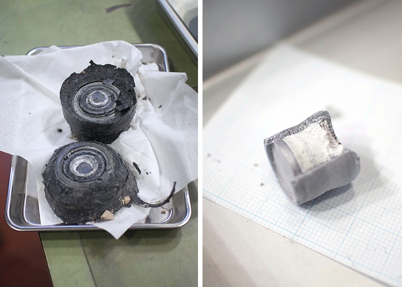
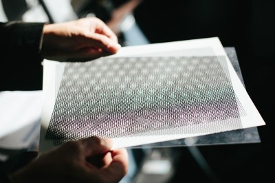
The synthesized hBN crystals, as well as the noncrystallized boron nitride powder, are contained in a molybdenum capsule.Credit: Mark Zastrow
It worked and Kim, Lee and Dean became the first external users of NIMS crystals for graphene research. It took Dean, in collaboration with doctoral students Andrea Young and Inanc Meric, a year to find a way to consistently handle graphene and hBN flakes in contact with each other. . But the results have been staggering. Based on NIMS hBN samples, graphene roughness was reduced by two-thirds compared to graphene on a silicon oxide substrate – and electron mobility was 10 to 100 times better.
The team presented its findings at the annual graphene week conference, held in April 2010 at the University of Maryland, College Park – and "all eyes have appeared," Kim said. "It was sensational." Everyone wanted to know how to get the hBN, including Geim, who received the Nobel Prize in physics that year for his work on graphene. He sent an email to Kim with a question: "Philip: what is the source?"
Taniguchi and Watanabe were suddenly inundated with inquiries and requests for samples. But when Geim, a Kim competitor, asked them, they hesitated to answer. "Things could have become complicated," says Taniguchi. "We made the crystal – they found the property." He asked Kim: would it be acceptable to provide other groups – including their direct competitors? "Of course," Kim said. "A small research group in Columbia should not monopolize your crystal," recalls Taniguchi.
Collaboration all around
Today, Taniguchi and Watanabe have agreements to supply more than 210 institutions worldwide. Taniguchi prepares the crystals for display in an office on the perimeter of the laboratory, where stacks of clear plastic trays containing sample batches are scattered around a microscope on a countertop. The current Taniguchi lot is numbered 942 – the last one in its archive, which goes back more than ten years. The total weight of the crystals in each package – containing four different samples from four cycles of the press – is about one gram. But this can keep a whole group of research for a year.
Taniguchi and Watanabe do not explicitly ask to be full co-authors on papers, they say. To receive the samples, users sign a Material Transfer Agreement with NIMS. Many researchers claim that the status of co-authors of the pair reflects the importance of the field's sample producers. "Without their samples, without their involvement, I do not think we can do what we are doing, so the sharing of authors is really deserved," says Kim.
The worst part of the procurement operation is the paperwork, Watanabe says. "It's a heavy burden – very heavy," he says. NIMS authors must submit individual reports to their supervisors when submitting a document, it is accepted and published. Watanabe, the junior partner and the most thorough of the two, takes charge of the task. He uses an application on his laptop to track the items and pre-impressions of the pair, which are now over 700.
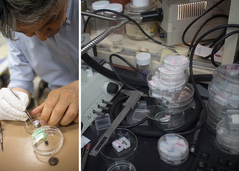
Kenji Watanabe prepares crystals of hexagonal boron nitride (hBN) (left); piles of plastic trays containing piles of hBN for display around the world.Credit: Mark Zastrow
In most studies, the interaction between Taniguchi and Watanabe is limited to providing the crystals and, they hope, to obtain information from these groups on the quality of the crystals. Everyone does not take the time to answer, says Taniguchi, to his disappointment. But their work with members of the original Columbia group – and the second generation groups that former Columbia students had created when they set up their own labs elsewhere – remains a real collaboration. "They have been phenomenal partners in this process," Dean said. "They have worked with us to provide boron nitride, but also to try to find ways to make things cleaner and create a variety of things that interest us."
After the presentation of Graphene Week in 2010, for example, a student of Pablo Jarillo-Herrero, named Kim, was the first person to request crystals from the Japanese pair. He is now leading the team at the Massachusetts Institute of Technology in Cambridge that reported last year superconductivity in twisted double layers of graphene1,2 – a configuration protected by two layers of Taniguchi and Watanabe hBN. And when physicist Rebeca Ribeiro-Palau left Dean's group in 2017 to head her own team at the Center for Nanosciences and Nanotechnology in Palaiseau, France, she immediately contacted the Japanese couple. "Establishing a collaboration with them was the first step, even before opening the lab," she says.
Graphene is not the only 2D material to benefit from hBN, adds Ribeiro-Palau. Layers of more complex materials, called transition metal dichalcogenides, for example, have also been stacked and twisted to alter their electronic properties, necessitating hBN again.7. "This is exactly what you need to encapsulate materials, protect them, give different properties, change the spacing between layers. We use boron nitride for almost everything, "said Ribeiro-Palau.
More and more evidence suggests that hBN can play more than a supporting role in such devices. The alignment of the hexagonal structure of hBN on one of the layers of twisted graphene can break the symmetry of graphene sheets, thus altering the interaction of electrons, according to separate pre-impressions reported this year by teams led respectively by David Goldhaber – Gordon of Stanford University in California. and Andrea Young, now at the University of California at Santa Barbara8,9.
Hexagonal boron nitride is increasingly recognized as a fascinating 2D material in its own right. Bathed by infrared light, hBN acts like a hyperlens: it can focus light and create sharper images than classical physics allows. And it has potential as a material that can emit unique photons – a useful function for quantum cryptographyten. Watanabe's discovery that the material might be useful as a UV laser continues to attract attention, and his main research goal remains to determine how this will happen.
Part of this work is carried out using hBN techniques grown according to methods producing lower quality samples, such as deposition of the crystal in a thin film from a chemical vapor, which does not require pressures. high. But for graphene researchers, it is the Taniguchi and Watanabe crystals that remain. "Over the years, we've tried four or five other hBN sources, all of which were garbage," says Geim. The shortage of high-purity hBN hampers progress in global graphene research, he says.
The other teams are starting to catch up. A group led by chemical engineer James Edgar of Kansas State University in Manhattan is about to achieve the quality needed to compete with Taniguchi and Watanabe processes, Geim notes. Edgar says it is not easy to replicate the work of the Japanese team because it has a costly and giant press. But his samples, made in a simpler – and much cheaper – process involving a furnace fed with boron nitride and a nickel-chromium solvent in powder form, are "as good or nearly as good" for the purposes of graphene research, he says. However, they currently have ten times more crystalline defects, or imperfections, in their structure.
Taniguchi, on the other hand, appreciates the prospect of challengers up to their crown and the chance to push each other to produce purer and more perfect crystals. "We are fighting to improve our systems," he said, "but we need many collaborators – and also competitors."
A career in crystal growth
This July, Taniguchi turned 60 – the age at which researchers retire at NIMS. It was a concern for Kim. "I told him," Hey, Takashi, the whole field of 2D research is in danger. So, we should do something! "Fortunately for the 2D field, NIMS granted a reprieve to Taniguchi: earlier this year, they promoted him to a fellow job, which allows him to work up to 65 years of age." . He has not yet developed a succession plan. or identified a protégé.
For the moment, he continues to run the press alone. Back in his lab, he prepares the next batch, number 943, by filling a new size-thimble sized capsule with white boron nitride disks the size of mints at the same time. breath. In between, he places a layer of barium nitride and other barium compounds, which dissolve with boron nitride and act as a solvent and catalyst to promote crystal growth and absorb impurities.
Taniguchi is careful about the exact recipe: it is about his secret sauce and he likes to change the composition of the barium layer from one batch to the other. "Using the same recipe every time is not so much fun," he says. For novice users, it will send basic crystals, but with long-time users, it wants feedback on every slight change in the process. By measuring the mobility of electrons in graphene, they can detect impurities in the underlying hBN with more sensitivity than Taniguchi and Watanabe can measure. At first no one complained of their crystals. According to Taniguchi, it's only been two years since researchers started reporting impurities that affect their results – pushing them to push the boundaries of the material. And that motivates Taniguchi to improve. "I'm a crystal producer," he says proudly.
He climbs onto the press platform, squatting into the jaws of the machine to place the new capsule. Back to the controls: a few taps on the keys and the lower anvil starts to come out of the ground to hit the center. While the red digital reading counts the distance, Taniguchi removes dirt from the console with a tissue.
Despite decades of work in the production of crystals in the press, much remains to be discovered about the fundamental physics of the process, he said. What's really going on inside this capsule when the press is tightening remains a mystery. "Nobody knows how to measure it, how to think about what's going on, how the crystal is developing. It's just imagination.
[ad_2]
Source link